A single sheet of atoms organized in a hexagonal lattice nanostructure makes up the carbon allotrope known as graphene. It is the term for a sheet of a single layer (monolayer) of carbon atoms that creates bonds in a recurring hexagonal pattern. Graphene typically exists as a powder composed of tiny, distinct sheets, each about the size of a sand grain. Graphene monolayers are piled on top of one another to create graphite. Given that, a typical carbon atom has a diameter of 0.33 nanometers, a sheet of graphite one millimeter thick contains about three million sheets of graphene. It is the strongest material known to humans.
Discovery Of Graphene
- P.R. Wallace began studying graphene theoretically in 1947 and used it as a textbook illustration for computations in solid-state physics. In addition to noticing the linear dispersion connection, he predicted the electrical structure.
- Russian physicist Professor Andre Geim developed an interest in graphene during 2002 and presented an assignment to a Ph.D. candidate to cut down a piece of graphite into as few layers as achievable. He was able to create a flake of graphite that was about 1,000 layers thick.
- Professors Andre Geim and Konstantin Novoselov, researchers at the University of Manchester, first discovered graphene in 2004. They used sticky tape to detach flakes from a lump of bulk graphite and discovered some were thinner than others. They were able to make flakes of graphite that were only one atom thick by continuously separating the graphite shards. This led to the isolation of graphene from graphite.
- Professors Geim and Novoselov were jointly awarded the Nobel physics prize in 2010 for their work on graphene.
Structure of Graphene
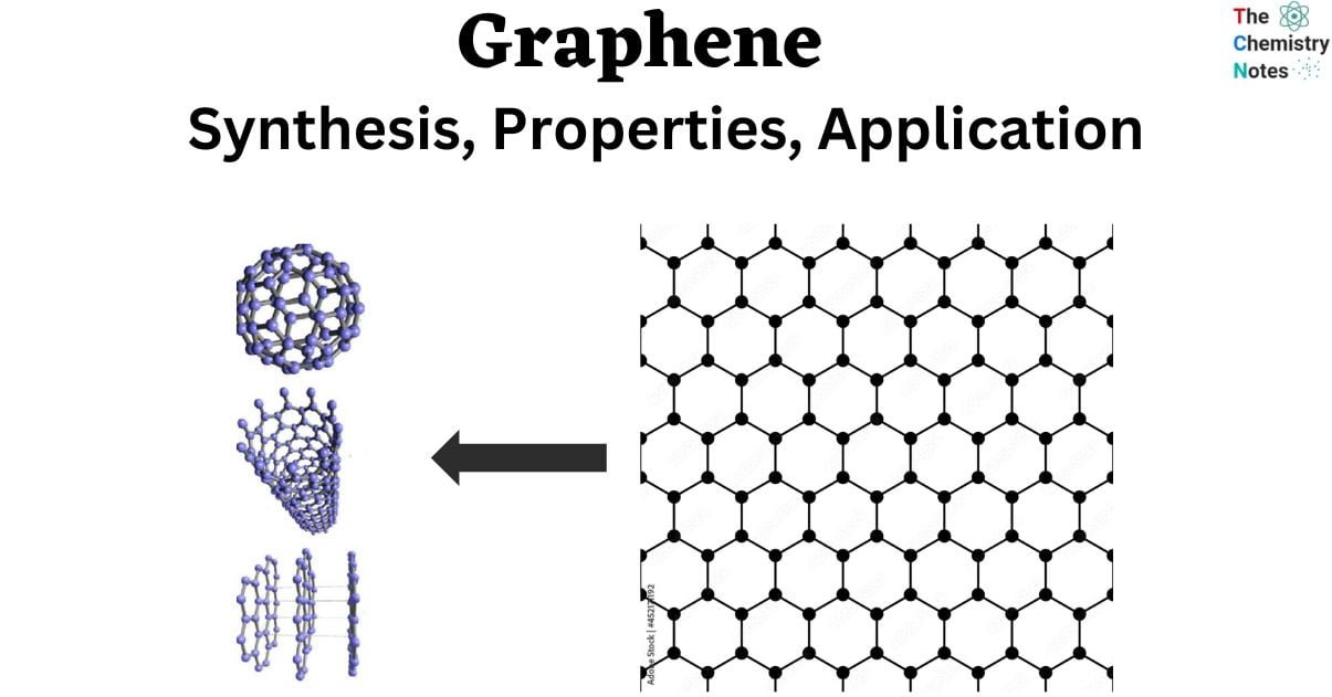
Graphene is one of the first and most well-known instances of a two-dimensional crystal. Graphene can be a parent form for many carbon structures, including the previously mentioned graphite, carbon nanotubes (which can be viewed as rolled-up sheets of graphene formed into tubes), and buckyballs (spherical structures with a cage-like structure made from graphene but with some hexagonal rings replaced by pentagonal rings).
When carbon atoms share sp2 electrons with their three nearby carbon atoms, they form a layer of honeycomb network with a planar shape, commonly known as monolayer graphene. The unit cell of a graphene crystal includes two carbon atoms, and the unit-cell vectors a1 and a2 have the same lattice constant of 2.46. The planar ring’s stability is due to electron resonance and delocalization.
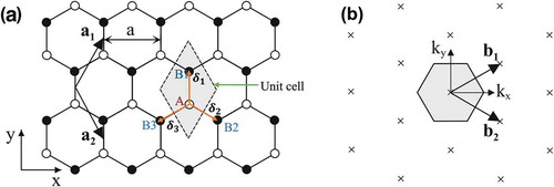
[Image Source: Springer-Verlag BerlinHeidelberg)
An out-of-plane bond is generated by 2pz orbitals that are perpendicular to the planar structure in a typical sp2 hybridization of two nearby carbon atoms on the graphene layer whereas an in-plane link is formed by the sp2 (2s, 2px, 2py) hybridized orbitals. The resulting covalent bond has a short interatomic length of 1.42, making it even stronger than diamond’s sp3 hybridized carbon-carbon bonds, giving monolayer graphene remarkable mechanical properties (for example, Young’s modulus of 1 TPa and an intrinsic tensile strength of 130.5 GPa. Due to the half-filled band that allows free-moving electrons, the conduction and valence bands with zero band gap form in monolayer graphene.
Furthermore, in bilayer and multilayer graphenes, the -bonds generate a weak van der Waals connection between adjacent graphene layers.
Properties of Graphene
Electronic properties
One of the reasons graphene is so appealing to molecular electronics researchers working in nanotechnology is because of its exceptional electrical conductivity. Because of the unusual way that the carbon atoms are arranged in graphene, electrons may readily go through it at very high speeds without encountering a major risk of scattering, conserving valuable energy that would otherwise be lost in other conductors.
Because the electrons don’t appear to slow down or localize, scientists have discovered that graphene can continue to conduct electricity even at the limit of supposedly zero carrier concentration. Additionally, it was discovered that they move much more quickly than electrons in other semiconductors.
Mechanical Properties
Graphene has amazing inherent mechanical capabilities, including its stiffness, strength, and toughness. They are caused by the sp2 bonds that create the hexagonal lattice and oppose various in-plane deformations.
Optical Characteristics
The ability of graphene to absorb 2.3% of white light is also a unique and intriguing attribute, especially given that it is only 1 atom thick. This is due to the electrons’ aforementioned electronic capabilities, which act as massless charge carriers with extremely high mobility.
Thermal Properties
The thermal conductivity of graphene is affected by diffusive and ballistic circumstances at higher and lower temperature ranges, respectively. The heat conductivity of graphene materials is greatly dependent on the quality of the graphene sheets
Chemical Properties
In terms of chemical reactions, pure graphene is rarely reactive. The chemical properties of graphene are heavily controlled by its surface features and layer thickness. Single layer graphene materials are more chemically reactive than multilayer graphene materials. Nitrene chemistry governs the reactivity of graphene materials.
Synthesis Of Graphene
Two-dimensional carbon-sp2 hybrids make up the substance known as graphene. It is essential to synthesize high-quality graphene due to its significant role in nanoelectronics. Depending on the intended size, purity, and efflorescence of the particular result, every procedure for manufacturing or extracting graphene is a graphene synthesis.
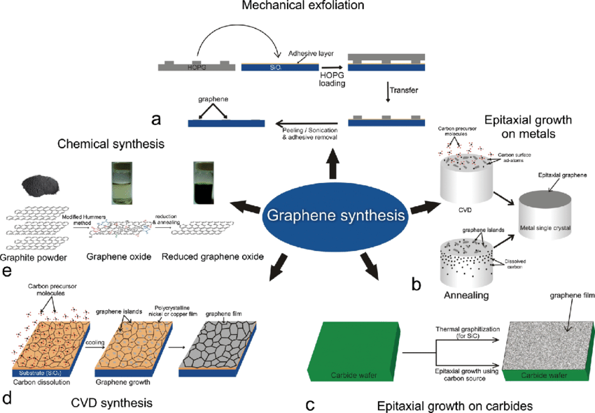
[Image source: http://dx.doi.org/10.1166/jnn.2011.5001]
These different ways to synthesize graphene are discussed here:
Peel-Off Method Or Mechanical Exfoliation
Graphene is created by pulling apart the layers of graphite with adhesive tape. This method leaves multiple layers of graphene after pulling it off, and after further peeling, it rips apart into a few graphene flakes. Then it is attached to a specific substrate (acetone) for removal, and the process is repeated to produce graphene flakes that are distinct in size and thickness and can be observed on SiO2/Si surfaces under a light microscope. This approach is slow and uneconomical. This approach can also be carried out using different materials, such as epoxy resin and transfer printing.
Electrochemical Exfoliation
Recently, an easy but highly productive approach to synthesizing large quantities of graphene has been discovered, which is known as electrochemical graphite exfoliation. This technique uses several graphites, including graphite foils, plates, rods, and powders, as electrodes in an aqueous or non-aqueous electrolyte, along with an electric current that causes the electrodes to expand. Depending on the amount of energy applied, an electrode might function as either cathodic (negative) or anodic (positive).
Arc Discharge Method
The anode and the cathode in the reaction chamber are immersed in either a liquid or a gas medium when using the arc discharge method. The medium is dissolved by passing off the electricity, which creates a high-temperature plasma (3727 °C–5725 °C) sufficient to sublime the precursor. Because a vacuum is utilized, this treatment is considered expensive. For cost-cutting in graphene production, the air is preferred to the hydrogen (H2) or helium (He) medium. Petroleum asphalt, a carbon-rich source, and water are utilized as mediums, reducing expenses. These advancements in arc discharge technology make the production of graphene cost-effective.
Pyrolysis Method
To create few-layer graphene, carbon atoms are synthesized on a metal surface. The thermal breakdown of silicon carbide (SiC) is one of the processes for graphene production. When temperatures are elevated, Si is desorbed, leaving a carbon atom that generates layers of graphene. The rapid production of graphene films on the mm scale at 750 °C on a thin film of nickel plated on a SiC substrate has substantially enhanced this approach.This approach, however, cannot be employed for large-scale graphene synthesis. The advantage of this approach is that it produces a high-purity graphene monolayer.
Chemical Vapor Deposition
Chemical vapor deposition comprises a chemical reaction where processed molecules are heated and converted to a gaseous state, known as the precursor. At high temperatures, a substrate is spread onto thermally disintegrating precursors, forming thin coatings of crystalline, solid, liquid, or gaseous precursors over the surface of the substrate. The chemical vapor deposition method is commonly used to deposit high-quality graphene onto transition-metal substrates such as nickel (Ni), palladium (Pd), ruthenium (Ru), and iridium (Ir). The initially tested substrate on which CVD development of large-area graphene was performed was nickel.
Oxidation-Reduction Method
This is one of the most common methods for producing graphene from graphite. There are four major techniques for converting graphite to graphene oxide: Brodie, Staudenmaier, Hofmann, and Hummer’s processes.Except for the utilization of different chemicals and better processes over the years, the technique is nearly identical. To keep production costs low, these processes require temperatures below 100 °C. The production of hazardous gases such as nitrogen dioxide (NO2) and dinitrogen tetroxide (N2O4) is one of the drawbacks of these approaches.
Applications of Graphene
With exceptional characteristics, graphene is a material employed in many different industrial applications. The following are some of the prominent applications of graphene.
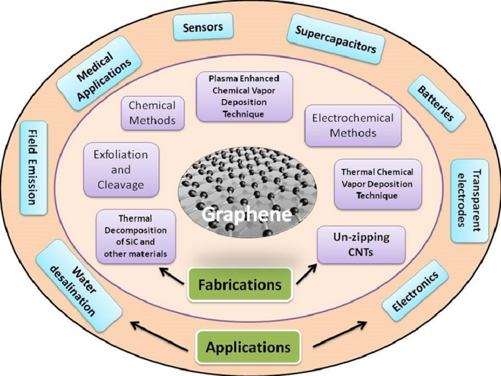
[Image Source: https://doi.org/10.1016/j.surfin.2017.08.004
Storage of energy and solar cells
Graphene-based nanomaterials have a wide range of promising uses in the energy sector. Here are a few recent examples: Graphene improves rechargeable battery energy capacity and charge rate; activated graphene makes superior supercapacitors for energy storage; graphene electrodes may lead to a promising approach for making inexpensive, lightweight, and flexible solar cells; and multifunctional graphene mats are promising substrates for catalytic systems.
Graphene and other direct band-gap monolayer materials, such as transition-metal dichalcogenides (TMDCs) and black phosphorus, have a high potential for use in low-cost, flexible, and highly efficient photovoltaic devices due to their excellent electron-transport properties and extremely high carrier mobility. They are the most promising advanced solar cell materials.
High-speed electronics
The conductivity property of electronics must be high in order for electronics devices to be efficient and effective in real-world applications. Graphene is one of the most sophisticated materials with great conductivity, making it perfect for high-speed electronics.
Biomedical applications
Graphene-based materials have lately gained popularity in pharmaceutical nanotechnology because to their unique chemical structure and physicochemical features, which include an ultra-high surface area, optical, thermal, and electrical conductivities, and good biocompatibility.
- Emerging applications include stem cell therapy, where graphene is employed as a biocompatible scaffold that promotes the proliferation of human mesenchymal stem cells (hMSCs) and speeds their differentiation into bone cells
- Furthermore, graphene-based nanomaterials can be functionalized with fluorescent and/or luminous diagnostic probes that can target ligands such as proteins, peptides, nucleic acids, antibodies, lipids, carbohydrates, and folic acid.
- Graphene-based nanomaterials have a lot of potential in pharmaceutical applications, such as improving drug circulation times, in target drug and gene delivery systems, acting as therapeutic agents and diagnostic tools, and graphene nano theranostic agents that combine both diagnostic and therapy approaches in a single system.
- Graphene-based photothermal agents could be used to trap and kill bacteria instead of antibiotics.
Thermoelectric applications
Thermal energy can be converted to electrical energy and vice versa using thermoelectric materials (TEM). Peltier coolers and thermoelectric power generators make extensive use of TEM. Graphene materials have outstanding thermoelectric capabilities, prompting industrialists to focus on using graphene in thermoelectric applications.
Face masks
Face masks have shown to be an effective tool in the fight against the COVID-19 epidemic. However, poor mask use or disposal may result in “secondary transmission.” A research team successfully created graphene face masks with an antibacterial efficacy of 80%, which can be increased to nearly 100% after 10 minutes of exposure to sunshine.
Data storage
One of the most important areas of research is data storage. Researchers are working on powerful small-size hard drives that can hold more data. Researchers hypothesized that substituting indium tin oxide electrodes with polymers and graphene oxide would result in write-read-read-rewrite characteristics. Graphene-based storage devices are ten times more powerful than today’s storage disks. Making compact storage devices is not a problem, but raising storage capacity levels is a critical effort. Graphene oxide device applications will make a significant difference in modern industrial environments.
Cloaking
The notion of plasmonic cloaking is based on the employment of a thin metamaterial cover to suppress scattering from a passive item. According to research, even a single layer of atoms with the intriguing conductivity qualities of graphene can provide this functionality in planar and cylindrical shapes. As a result, a single layer of graphene is the thinnest feasible invisibility cloak.
Environmental Applications
Graphene and its derivatives are critical in the removal of harmful contaminants from the environment.
- Graphene is employed as a physical support for iron oxide nanoparticles, increasing surface area and the number of metal ion binding sites. Using magnetic characteristics, magnetically active iron oxide can be easily extracted from solution and can adsorb metal ion pollutants.
- The adsorption of CO2 and H2 on the graphene surface was studied, and it was discovered that a single layer of graphene has the highest adsorption of 37.93%. The surface of graphene may be adjusted to selectively absorb gaseous contaminants.
Coating
Graphene-coated objects can fulfill a variety of functions. For example, researchers have demonstrated that graphene sheets can be used to make a superhydrophobic coating material with stable superhydrophobicity under both static and dynamic (droplet impact) conditions, resulting in exceptionally water repellent structures.
Supercapacitors
Supercapacitors are essential energy storage devices that use a large internal surface area to retain charge and provide larger currents than standard capacitors. Because of its increased internal area, graphene has the potential to be a great material for supercapacitors. More research is being conducted to develop graphene-based supercapacitors for a variety of sophisticated applications.
References
- https://www.bbc.co.uk/bitesize/guides/zfsct39/revision/6
- Bhuyan, M.S.A., Uddin, M.N., Islam, M.M. et al. Synthesis of graphene. Int Nano Lett 6, 65–83 (2016). https://doi.org/10.1007/s40089-015-0176-1
- Santhiran, Anuluxan, Poobalasuntharam Iyngaran, Poobalasingam Abiman, and Navaratnarajah Kuganathan. 2021. “Graphene Synthesis and Its Recent Advances in Applications—A Review” C 7, no. 4: 76. https://doi.org/10.3390/c7040076
- https://www.repsol.com/en/energy-and-the-future/technology-and-innovation/graphene/index.cshtml
- https://www.graphenea.com/pages/graphene-uses-applications
- https://www.graphene.manchester.ac.uk/learn/applications/
- https://www.graphene-info.com/graphene-applications
- Structure of graphene and its disorders: a review: https://doi.org/10.1080/14686996.2018.1494493
