Nanolithography is a subfield of nanotechnology that refers to the process of imprinting , writing, or etching patterns on a tiny scale to build extremely small structures. Nanolithography is primarily used in a variety of technological fields ranging from electronics to biomedicine. Nanolithography is a versatile and effective technology for creating nanoscale patterns.

The term nanolithography is derived from the Greek words “nanos” (dwarf), “lithos” (rock or stone), and “graphein” (to write). As a result, the literal translation is “tiny writing on stone,” but when this term is coupled with nanotechnology, one gets something different. Nanolithography is employed in the nanofabrication of cutting-edge semiconductor integrated circuits (nanocircuitry), nanoelectromechanical systems (NEMS), and nearly any other basic application in nano research.
What is Nanolithography?
Nanolithography is the branch of nanotechnology dealing with the study and implementation of nanofabrication of nanometer-scale structures, which means nanopatterning with at least one lateral dimension between the size of an individual atom and about 100 nm.
Nanolithography is employed in the nano manufacturing of cutting-edge semiconductor integrated circuits (nanocircuitry), nano electromechanical systems (NEMS), and almost any other basic application across many scientific disciplines in nano research.
This method has the potential to be useful in the nanofabrication of various semiconducting Integrated Circuits (ICs), NEMS, and other research applications. It is also possible to modify semiconductor devices at the nanoscale (in the 10-9 meter range).
Nanolithography Techniques
For patterning at the nanoscale, several lithographic techniques are utilized. Some of the Nanolithography techniques are:
- Photolithography
- Electron beam lithography (EBL)
- X-ray lithography
- Extreme ultraviolet lithography (EUVL)
- Light coupling nanolithography (LCM)
- Scanning probe microscope lithography (SPM)
- Nanoimprint lithography
- Dip-Pen nanolithography
Photolithography
Photolithography techniques used in nanolithography are quite similar to those used in conventional lithography for image and printing output. Photolithography is widely used to manufacture computer chips. This method permits hundreds of chips to be produced on a single silicon wafer at the same time. Photolithography can create features as small as 50nm. In the mass manufacture of microelectronics and semiconductor devices, photolithography is the most widely utilized process. It is distinguished by high production throughput as well as small-sized pattern features.
Electron Beam Lithography
Electron Beam Lithography (EBL) etching a pattern of nano-sized features by scanning a closely focused beam of electrons across the surface of a substrate. EBL can create features as small as 20nm, but it is both expensive and time demanding. A lithographic procedure that would take 5 minutes with photolithography would take around 5 hours with EBL.
X-ray Lithography
X-ray lithography is similar to photolithography and extreme ultraviolet lithography, except it employs a mask constructed of an X-ray transparent material with a pattern of high Z material either etched or deposited on it. A parallel beam of X-rays is used to expose the substrate resist. The etched pattern’s resolution is determined by the mask’s characteristics and the exposure control.
Extreme Ultraviolet Lithography
Extreme Ultraviolet Lithography (EUVL) is similar to regular photolithography in that it burns a pattern into a silicon wafer using intense beams of ultraviolet light reflected from a circuit design pattern. Unlike photolithography, which employs a lens system to concentrate light, extreme ultraviolet light is reflected through a sequence of mirrors in EUVL. The current limiting issue in EUVL is the ability to build mirrors with adequate precision, but if this problem is overcome, resolutions below 30nm are expected.
Light Coupling Nanolithography
Another version on photolithography is light coupling nanolithography (LCM). A polymer mask is placed in contact with the photoresist in LCM. Where exposure is required, transparent patches protrude through the topographically designed mask. The contrast of masked areas can be improved further by applying a thin gold overlay.
Scanning Probe Microscope Lithography
Microscope with Scanning Probe The electric field at the tip of a scanning probe microscope is used in lithography (SPM) to oxidize material in a specified pattern. After that, the oxidized material can be removed via preferred etching.
Nanoimprint Lithography
Nanoimprint lithography is a simple procedure that embosses the resist with the desired design using a mould. After embossing the resist, the compressed resist material is removed with anisotropic etching, exposing the substrate. Nanoimprint lithography can achieve resolutions of less than 10nm while maintaining high throughput and cheap cost. The development of the mould itself is the present obstacle to production at these resolutions. Self-assembly nanomanufacturing may hold the key to overcoming this barrier.
Dip-Pen Nanolithography
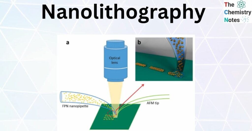
Dip-Pen Nanolithography (DPN) is a direct write lithographic process that builds a pattern on the substrate material rather than etching it away using an atomic force microscope (AFM). Similarly to how a traditional dip pen takes up ink from an ink well and then writes on paper, molecules are picked up from a reservoir on the end of the AFM tip and deposited on the surface of the substrate via a solvent or water. DPN can produce patterns with resolutions as low as 40nm.
Nanolithography techniques and hybrid approaches
New procedures or techniques that have enlarged the frontiers for nanofabrication have enhanced the field of nanolithography in recent years.
To encompass all options, the term hybrid can be used in this sense to mean:
(a) The use of two or more top-down nanolithography techniques to pattern a material or fabricate a nanodevice;
(b) The combination of a top-down nanolithography technique with a bottom-up nanofabrication process to achieve a specific nanopatterning process or nanodevice, or the unconventional use of a top-down nanolithography or a bottom-up nanofabrication technique with thin-film or other growth techniques with the goal of nanopatterning.
Some examples are: stencil lithography, nanosphere/colloidal lithography, roll-to-roll lithography , Talbot lithography, soft x-ray lithography using resists or precursors, proton-beam lithography, plasmonic lithography, ice lithography, fountain-pen nanolithography, crack lithography, grain-boundary lithography.
Stencil Lithography
A thin plate with specified apertures is placed in close proximity to the substrate and used in conjunction with material evaporation. Except for the apertures, the evaporated material is stopped on the top surface of the stencil mask. As a result, the material grows with precise patterns dictated by the stencil mask.
Nanopatterned materials can be generated at the wafer scale in a single shot using proper stencil masks. Resolution down to 20 nm has been achieved, and it may be utilized on atypical substrates such as cantilevers, however the technology has several drawbacks such as shadow deposition beneath the stencil mask and longevity concerns due to stencil breakdown.
Nanosphere/colloidal lithography
This term refers to a group of techniques that use a solution of nanoparticles to generate a very thin layer on the substrate of interest and serve as a sacrificial layer during the nanopatterning process. Because of their interaction, nanoparticles can self-organize, forming a thin layer with gaps between them. Natural lithography was the initial name for the method. Given the colloidal particles’ monodisperse nature and hydrophilic nature, they create a colloidal crystal with ordered holes through which the material of interest will penetrate and be deposited on the substrate. Polystyrene latex nanospheres, for example, can be employed.
The possibility for large-area patterning, simplicity, good resolution, and the flexibility to be integrated with other lithography techniques are all advantages of this approach. However, the process creates challenges due to the limited forms accessible for the patterned functional material, the long-range order of the nanopatterns, and the occurrence of point defects.
Applications of Nanolithography
Nanolithography is gaining popularity for transdisciplinary applications, particularly in biology and medicine. Nanolithography comes into play in two ways. For starters, it can be used to create electrical devices that provide a digital readout of a specific measurement or allow the application of a specific external action. Second, given the micrometric or nanometric scale of items like bacteria, viruses, proteins, DNA, and so on, artificial objects of comparable size are relevant for interacting with those entities. This has resulted in a number of applications in the following areas:
- bionsensing and medical diagnosis
- DNA and protein sequencing
- microfluidic and lab-on-a-chip devices
- medical treatments (drug delivery, hyperthermia, mechanical treatment, etc)
- medical imaging techniques
- neuroscience
- scaffolds for tissue growth and cell differentiation
- It has applications in the fabrication of integrated circuits and parts for semiconductor technology, where the capacity to manufacture the most compact transistors and circuits enables the fabrication of smaller devices while also enhancing the power efficiency and performance of the components.
- Furthermore, advances in lithography techniques have made it possible to build complex structures suitable for microelectromechanical or nanoelectromechanical systems (MEMS or NEMS) devices.
- While these small devices have already been used as pH sensors and transistors, there are other potential for future development of this technology, including the use of these devices for drug administration.
- Given its high throughput, optical lithography was determined to be the best technology for this fabrication. Furthermore, it could meet the increasing resolution requirements of each new generation of electronic equipment.
- The advancement of flexible electronics has pushed the usage of nanolithography into new emerging applications in biomedicine (biopsy diagnosis, optical stimulation implants, cardiac patches, brain mapping), flexible LEDs, flexible touch displays, and strain and temperature sensors.
- More futuristic, but rapidly approaching reality, flexible electronic components are being created to achieve human-machine interaction, such as in the artificial retina.
References
- R. C. Davis et al., Chemomechanical Surface Patterning and Functionalization of Silicon Surfaces Using an Atomic Force Microscope, Appl. Phys. Lett. 82 (5): 808-810 (2003). Related article
- A. Hatzor-de Picciotto, A. D. Wissner-Gross, G. Lavallee, P. S. Weiss (2007). “Arrays of Cu(2+)-complexed organic clusters grown on gold nano dots”. Journal of Experimental Nanoscience 2: 3-11.
- FuL2003Dip-Pen Patterning of magnetic materials. Nano Lett., 3757760
- 5.IvanisevicA2001Dip-pen nanolithography on semiconductor surfaces. J. Am. Chem. Soc. 12378877889
- Colson P, Henrist C and Cloots R 2013 Nanosphere lithography: a powerful method for the controlled manufacturing of nanomaterials J. Nanomater. 2013 948510
- Piner R D, Zhu J, Xu F and Hong S 1999 ‘Dip-Pen’ nanolithography Science 283 661–4
